CPU & GPU - The Basics
A digestible high-level overview of what happens in The Die

🧑💻 Research & Engineering - LLM Inference & High Performance systems. |📍Berlin 🇩🇪 | 📚 https://venkat.eu | 💬 https://twitter.com/Venkat2811
Introduction
In this article, we'll go through some fundamental low level details to understand why GPUs are good at Graphics, Neural Network and Deep Learning tasks and CPUs are good at wide number of sequential, complex general purpose computing tasks. There were several topics that I had to research and get a bit more granular understanding for this post, some of which I will be just mentioning in passing. It is done deliberately to focus just on the absolute basics of CPU & GPU processing.
Von Neumann Architecture
Earlier computers were dedicated devices. Hardware circuits and logic gates were programmed to do specific set of things. If something new had to be done, circuits needed to be rewired. "Something new" could be as simple as doing mathematical calculations for two different equations. During WWII, Alan Turing was working on a programmable machine to beat Enigma machine and later published "Turing Machine" paper. Around the same time, John von Neumann and other researchers were also working on idea which fundamentally proposed:
Instruction and data should be stored in shared memory (Stored program).
Processing and memory units should be separate.
Control unit takes care of reading data & instructions from memory to do calculations using processing unit.
The Bottleneck
Processing bottleneck - Only one instruction and its operand can be at a time in a processing unit (physical logic gate). Instructions are executed sequentially one after another. Over the years, focus and improvements has been in making processors smaller, faster clock cycles, increasing number of cores.
Memory bottleneck - As processors grew faster and faster, speed and amount of data that could be transferred between memory and processing unit became a bottleneck. Memory is several order slower than CPU. Over the years, focus and improvements has been in making memory denser and smaller.
CPUs
We know that everything in our computer is binary. String, image, video, audio, OS, application program, etc., are all represented as 1s & 0s. CPU architecture (RISC, CISC, etc.,) specifications have instruction sets (x86, x86-64, ARM, etc.,), which CPU manufacturers must comply with & is available for OS to interface with hardware.
OS & application programs including data are translated into instruction set and binary data for processing in the CPU. At chip level, processing is done at transistors and logic gates. If you execute a program to add two numbers, addition (the "processing") is done at logic gate in the processor.
In CPU as per Von Neumann architecture, when we are adding two numbers, a single add instruction runs on two numbers in the circuit. For a fraction of that millisecond, only add instruction was executed in (execution) core of the processing unit ! This detail always fascinated me.
Core in a modern CPU
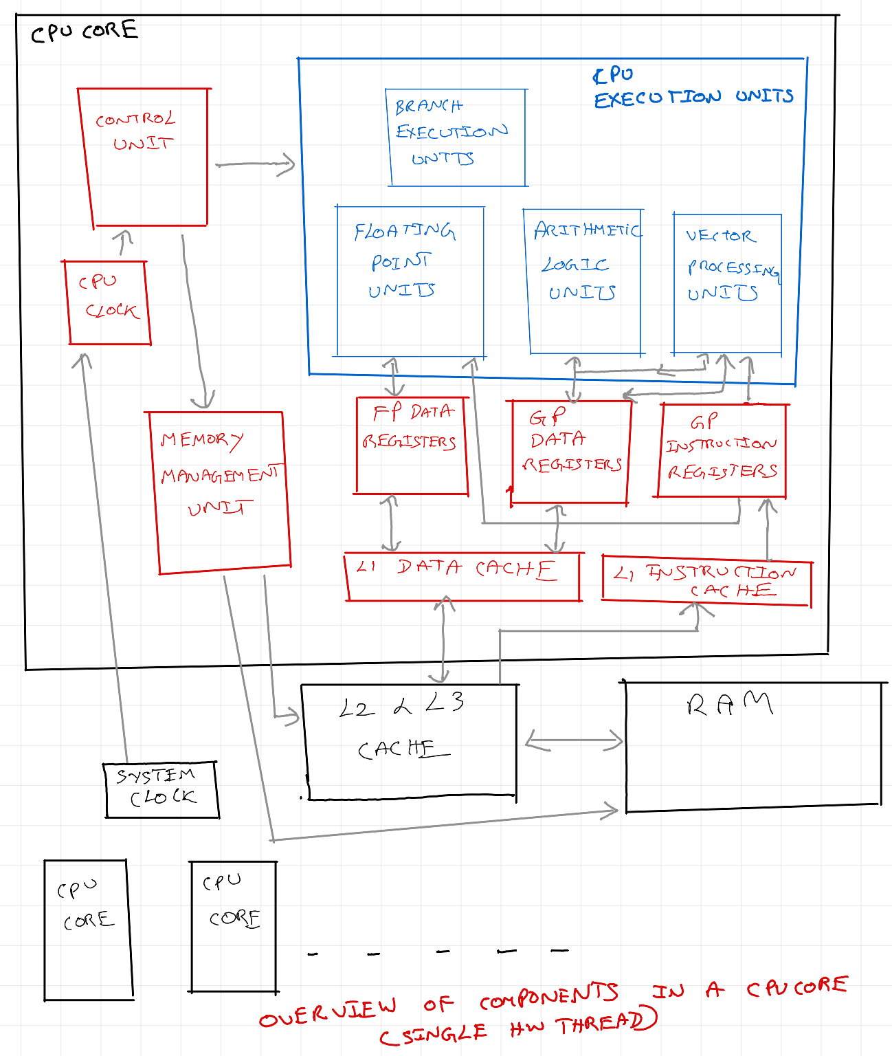
The components in the above diagram are self evident. For more details and detailed explanation refer to this excellent article. In modern CPUs, a single physical core can contain more than one integer ALU, floating-point ALU, etc., Again, these units are physical logic gates.
We need to understand 'Hardware Thread' in CPU core for better appreciation of GPU. A hardware thread is an unit of compute that can be done in execution units of a CPU core, every single CPU clock cycle. It represents the smallest unit of work that can be executed in a core.
Instruction cycle
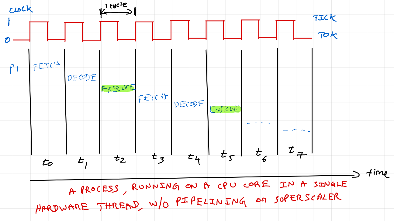
The above diagram illustrates CPU instruction cycle / machine cycle. It is a series of steps that CPU performs to execute a single instruction (eg: c=a+b).
Fetch: Program counter (special register in CPU core) keeps track of which instruction must be fetched. Instruction is fetched and stored in instruction register. For simple operations, corresponding data is also fetched.
Decode: Instruction is decoded to see operator and operands.
Execute: Based on the operation specified, appropriate processing unit is chosen and executed.
Memory Access: If instruction is complex or additional data is needed (several factors can cause this), memory access is done before execute. (Ignored in above diagram for simplicity). For a complex instruction, initial data will be available in data register of compute unit, but for complete execution of instruction, data access from L1 & L2 cache is required. This means could be a small wait time before compute unit executes and the hardware thread is still holding compute unit during wait time.
Write Back: If execution produces output (eg: c=a+b), output is written back to register / cache / memory. (Ignored in above diagram or anyplace later in the post for simplicity)
In the above diagram, only at t2 compute is being done. Rest of the time, core is just idle (we are not getting any work done).
Modern CPUs have HW components which essentially enables (fetch-decode-execute) steps to happen concurrently per clock cycle.A single hardware thread can now do computation in every clock cycle. This is called as instruction pipelining.
Fetch, Decode, Memory Access, Write Back are done by other components in a CPU. For lack of a better word, these are called "pipeline threads". Pipeline thread becomes hardware thread when it is in execute stage of an instruction cycle.
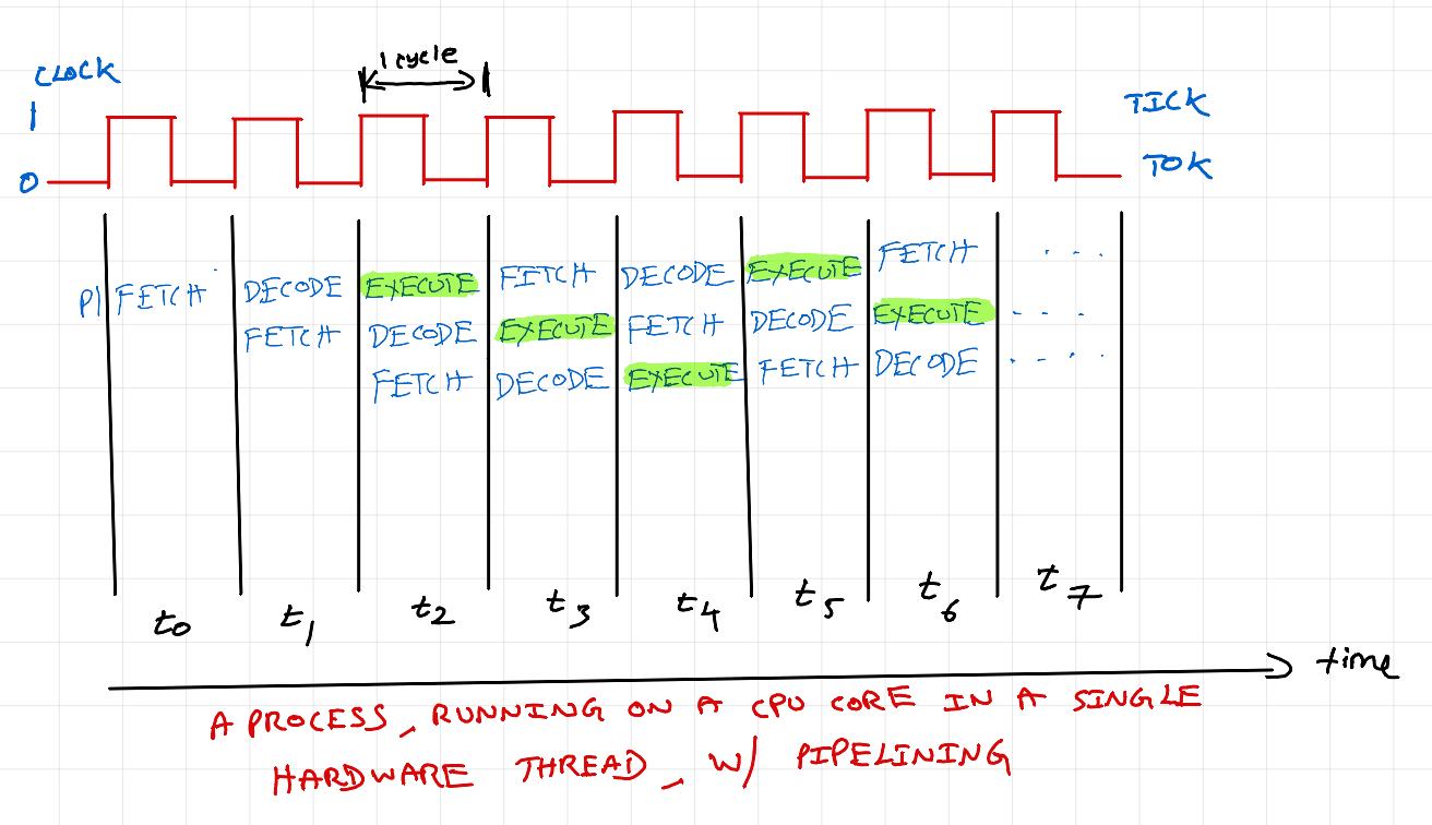
As you can see, we get compute output every cycle from t2. Previously, we got compute output once every 3 cycle. Pipelining improves compute throughput. This is one of the techniques to manage processing bottleneck in Von Neumann Architecture. There are also other optimizations like out of order execution, branch prediction, speculative execution, etc.,
Hyper-Threading
This is the last concept I want to discuss in CPU before we conclude and move on to GPUs. As the clock speeds increased, the processors also got so fast and efficient. With increase in application (instruction set) complexity, CPU compute cores were underutilized and it was spending more time waiting on memory access.
So, we are seeing memory bottleneck. Compute unit is spending time on memory access and not doing any useful work. Memory is several order slower than CPU and gap is not going to close anytime soon. The idea was to increase memory bandwidth in some units of a single CPU core and keep data ready to utilize the compute units when it is awaiting memory access.
Hyper-threading was made available in 2002 by Intel in Xeon & Pentium 4 processors. Prior to hyper-threading there was only one hardware thread per core. With hyper-threading, there will be 2 hardware threads per core. What does it mean ? Duplicate processing circuit for some registers, program counter, fetch unit, decode unit, etc.

The above diagram just shows new circuit elements in a CPU core with hyper threading. This is how a single physical core is visible as 2 cores to the Operating System. If you had a 4 core processor, with hyper-threading enabled, it is seen by OS as 8 cores. Obviously, L1 - L3 cache size will increase to accommodate additional registers. Note that the execution units are shared.
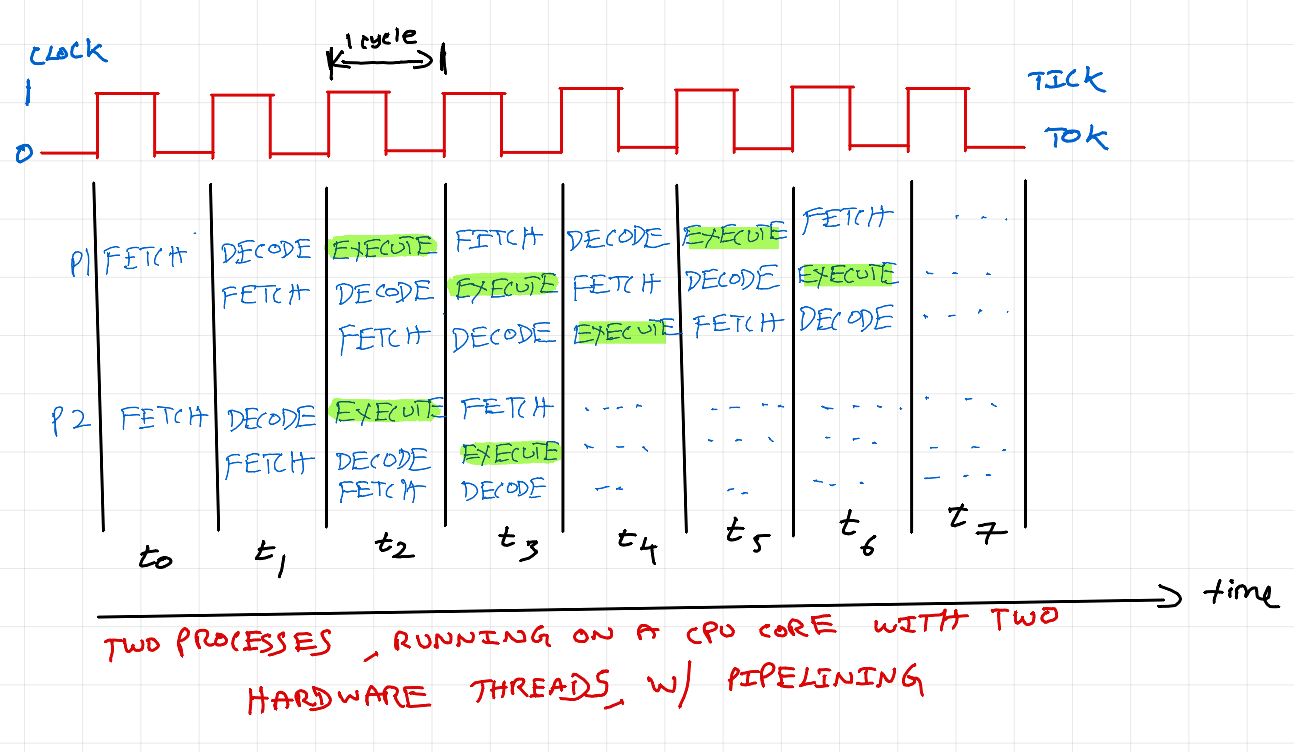
Assume we have processes P1 and P2 doing a=b+c, d=e+f, this can execute concurrently in a single clock cycle because of HW threads 1 and 2. Witch single HW thread as we saw earlier, this would not be possible. Here we are increasing memory bandwidth within a core by adding additional Hardware Thread so that, the processing unit can be utilized efficiently. This improves compute concurrency.
Some interesting scenarios:
CPU has only one integer ALU. One HW Thread 1 or HW Thread 2 must wait for one clock cycle and proceed with compute in next cycle.
CPU has one integer ALU and one floating point ALU. HW Thread 1 and HW Thread 2 can do addition concurrently using ALU and FPU respectively.
All available ALUs are being utilized by HW Thread 1. HW Thread 2 must wait until ALU is available. (Not applicable for the addition example above, but can happen with other instructions).
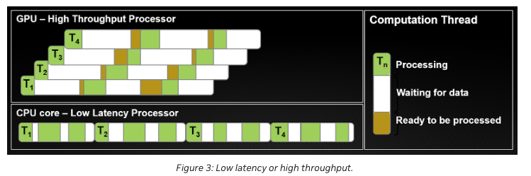
Why CPU is so good at traditional desktop / server computing ?
High clock speeds - Higher than GPU clock speeds. Combining this high speed with instruction pipelining, CPUs are extremely good at sequential tasks. Optimized for latency.
Diverse applications & computation needs - Personal computer and servers have wide range of applications and computation needs. This results in complex instruction set. CPU has to be good at several things.
Multitasking & Multi processing - With so many apps in our computers, CPU workload demands context switching. Caching systems and memory access is setup to support this. When a process is scheduled in CPU hardware thread, it has all necessary data ready and executes compute instructions quickly one by one.
CPU Drawbacks
Check this article & also try the Colab notebook. It shows how matrix multiplication is a parallelizable task and how parallel compute cores can speedup the calculation.
Extremely good at sequential tasks but not good at parallel tasks.
Complex instruction set and complex memory access pattern.
CPU also spends lots of energy on context switching, control unit activities in addition to compute
Key Takeaways
Instruction pipelining improves compute throughput.
Increasing memory bandwidth improves compute concurrency.
CPUs are good at sequential tasks (optimized for latency). Not good at massively parallel tasks as it needs large number of compute units and hardware threads which are not available (not optimized for throughput). These are not available because CPUs are built for general purpose computing and have complex instruction sets.
GPUs
As computing power increased, so did the demand for graphics processing. Tasks like UI rendering and gaming require parallel operations, driving the need for numerous ALUs and FPUs at the circuit level. CPUs, designed for sequential tasks, couldn't handle these parallel workloads effectively. Thus, GPUs were developed to fulfill the demand for parallel processing in graphics tasks, later paving the way for their adoption in accelerating deep learning algorithms.
I would highly recommend:
Watching this video that explains parallel tasks involved in Video Games rendering.
Reading this blog post to understand parallel tasks involved in a transformer. There are other deep learning architectures like CNNs, RNNs as well. Since LLMs are taking over the world, high level understanding of parallelism in matrix multiplications required for transformer tasks would set a good context for the remainder of this post. (At a later time, I plan to fully understand transformer & share a digestible high-level overview of what happens in transformer layers of a small GPT model.)
Example CPU vs GPU spec
Cores, hardware threads, clock speed, memory bandwidth, and on chip memory of CPUs & GPUs differ significantly. Example:
Intel Xeon 8280 has:
2700 MHz base and 4000 MHz at Turbo
28 cores and 56 hardware threads
Overall pipeline threads: 896 - 56
L3 Cache: 38.5 MB (shared by all cores) L2 Cache: 28.0 MB (divided among the cores) L1 Cache: 1.375 MB (divided among the cores)
Register size is not publicly available
Max Memory: 1TB DDR4, 2933 MHz, 6 channels
Max Memory Bandwidth: 131 GB/s
Peak FP64 Performance = 4.0 GHz 2 AVX-512 units 8 operations per AVX-512 unit per clock cycle * 28 cores = ~2.8 TFLOPs [Derived using: Peak FP64 Performance = (Max Turbo Frequency) (Number of AVX-512 units) (Operations per AVX-512 unit per clock cycle) * (Number of cores)]
- This number is used for comparison with GPU as getting peak performance of general purpose computing is very subjective. This number is a theoretical max limit which means, FP64 circuits are being used to its fullest.
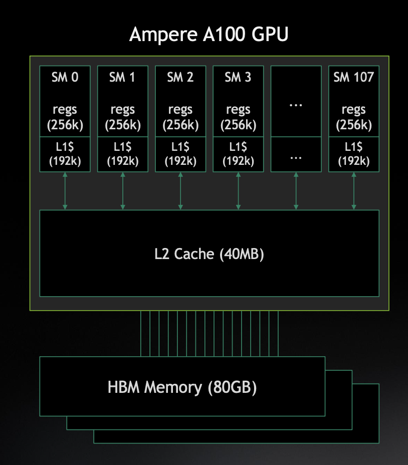
Nvidia A100 80GB SXM has:
1065 MHz base and 1410 MHz at Turbo
108 SMs, 64 FP32 CUDA cores (also called as SPs) per SM, 4 FP64 Tensor cores per SM, 68 hardware threads (64 + 4) per SM
- Overall per GPU: 6912 64 FP32 CUDA cores, 432 FP 64 Tensor cores, 7344 (6912 + 432) hardware threads
Pipeline threads per SM: 2048 - 68 = 1980 per SM
Overall pipeline threads per GPU: (2048 x 108) - (68 x 108) = 21184 - 7344 = 13840
L2 Cache: 40 MB (shared among all SMs) L1 Cache: 20.3 MB in total (192 KB per SM)
Register size: 27.8 MB (256 KB per SM)
Max GPU Main Memory: 80GB HBM2e, 1512 MHz
Max GPU Main Memory Bandwidth: 2.39 TB/s
Peak FP64 Performance = 19.5 TFLOPs [using only all FP64 Tensor cores]. Lower value of 9.7 TFLOPs when only FP64 in CUDA cores are used. This number is a theoretical max limit which means, FP64 circuits are being used to its fullest.
Core in a modern GPU
Terminologies we saw in CPU doesn't always translate directly to GPUs. Here we'll see components and core NVIDIA A100 GPU. One thing that was surprising to me while researching for this article was that CPU vendors don't publish how many ALUs, FPUs, etc., are available in execution units of a core. NVIDIA is very transparent about number of cores and CUDA framework gives complete flexibility & access at circuit level.
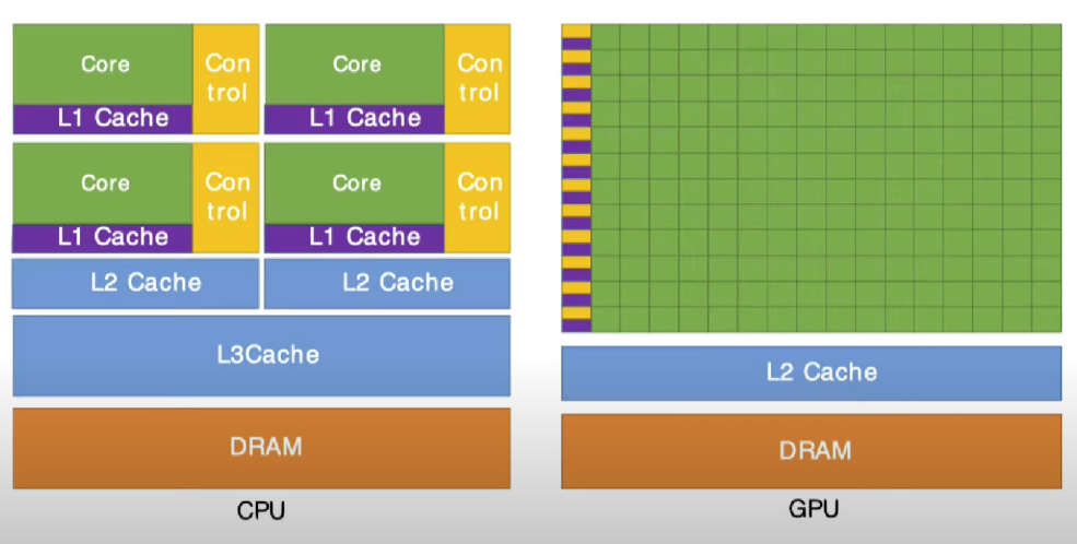
In the above diagram in GPU, we can see that there is no L3 Cache, smaller L2 cache, smaller but a lot more control unit & L1 cache and large number of processing units.
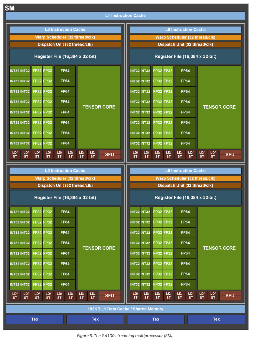
Here are GPU components in the above diagrams and their CPU equivalent for our initial understanding. I haven't done CUDA programming, so comparing it with CPU equivalents helps with initial understanding. CUDA programmers understand this very well.
Multiple Streaming Multiprocessors <> Multi Core CPU
Streaming Multiprocessor (SM) <> CPU Core
Streaming processor (SP)/ CUDA Core <> ALU / FPU in execution units of a CPU Core
Tensor Core (capable doing 4x4 FP64 operations on a single instruction) <> SIMD execution units in a modern CPU core (eg: AVX-512)
Hardware Thread (doing compute in CUDA or Tensor Cores in a single clock cycle) <> Hardware Thread (doing compute in execution units [ALUs, FPUs, etc.,] in a single clock cycle)
HBM / VRAM / DRAM / GPU Memory <> RAM
On-chip memory/SRAM (Registers, L1, L2 cache) <> On-chip memory/SRAM (Registers, L1, L2, L3 cache)
- Note: Registers in a SM are significantly larger than Registers in a core. Because of high number of threads. Remember that in hyper-threading in CPU, we saw increase in no of registers but not compute units. Same principle here.
Moving data & memory bandwidth
Graphics and deep learning tasks demand SIM(D/T) [Single instruction multi data / thread] type execution. i.e., reading and working on large amounts of data for a single instruction.
We discussed instruction pipelining and hyper-threading in CPU and GPUs also have capability. How it is implemented and working is slightly different but the principles are the same.
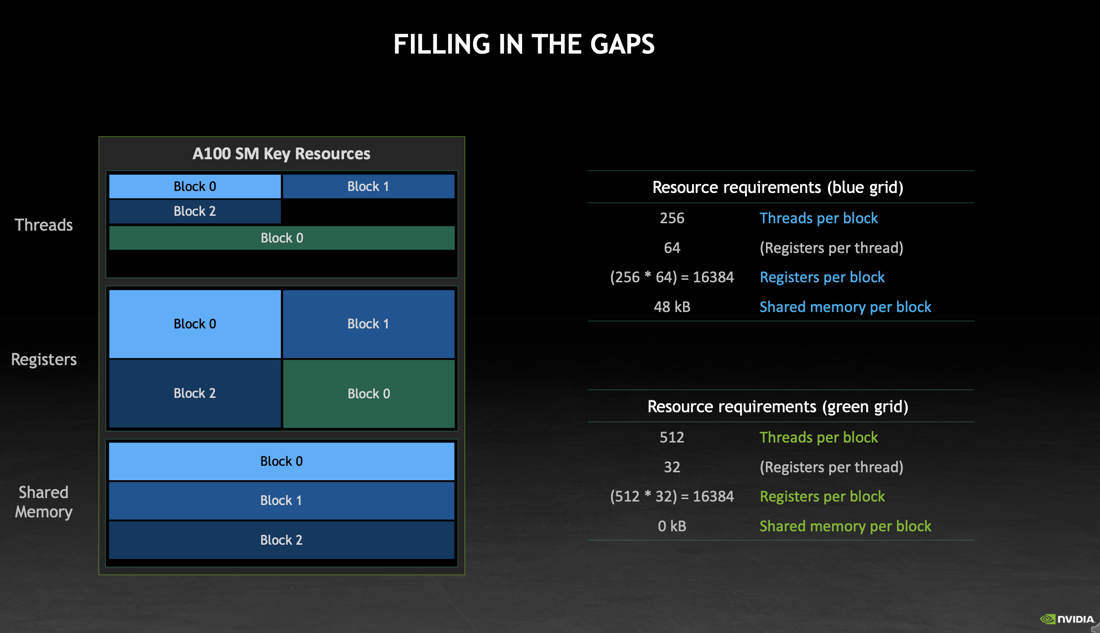
Unlike CPUs, GPUs (via CUDA) provide direct access to Pipeline Threads (fetching data from memory and utilizing the memory bandwidth). GPU schedulers work first by trying to fill compute units (includes associated shared L1 cache & registers for storing compute operands), then "pipeline threads" which fetch data into registers and HBM. Again, I want to emphasize that CPU app programmers don't think about this, and specs about "pipeline threads" & number of compute units per core is not published. Nvidia not only publishes these, but also provides complete control to programmers.
I will go into more details about this in a dedicated post about CUDA programming model & "batching" in model serving optimization technique where we can see how beneficial this is.
The above diagram depicts hardware thread execution in CPU & GPU core. Refer "memory access" section we discussed earlier in CPU pipelining. This diagram shows that. CPUs complex memory management makes this wait time small enough (few clock cycles) to fetch data from L1 cache to registers. When data needs to be fetched from L3 or main memory, the other thread for which data is already in register (we saw this in hyper-threading section) get's control of execution units.
In GPUs, because of over subscription (high number of pipeline threads & registers) & simple instruction set, large amount of data is already available on registers pending execution. These pipeline thread waiting for execution become hardware threads and do the execution as often as every clock cycle as pipeline threads in GPUs are lightweight.
Bandwidth, Compute Intensity & Latency
What's over goal?
Fully utilize hardware resources (compute units) every clock cycle to get the best out of GPU.
To keep the compute units busy, we need to feed it enough data.

This is the main reason why latency of matrix multiplication of smaller matrices are the same more or less in CPU & GPU. Try it out.
Tasks needs to be parallel enough, data needs to be huge enough to saturate compute FLOPs & memory bandwidth. If a single task is not big enough, multiple such tasks needs to be packed to saturate memory and compute to fully utilize the hardware.
Compute Intensity = FLOPs / Bandwidth. i.e., Ratio of amount of work that can be done by the compute units per second to amount of data that can be provided by memory per second.
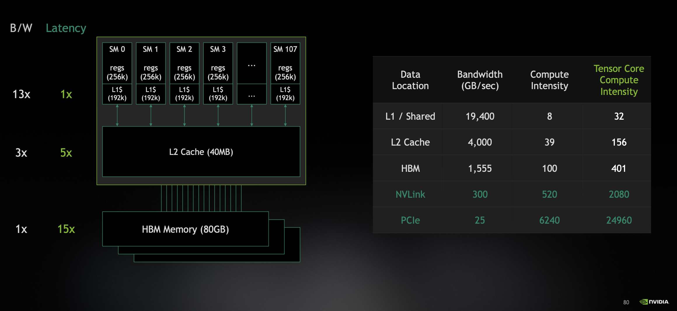
In above diagram, we see that compute intensity increases as we go to higher latency and lower bandwidth memory. We want this number to be as small as possible so that compute is fully utilized. For that, we need to keep as much as data in L1 / Registers so that compute can happen quickly. If we fetch single data from HBM, there are only few operations where we do 100 operations on single data to make it worth it. If we don't do 100 operations, compute units were idle. This is where high number of threads and registers in GPUs come into play. To keep as much as data in L1/Registers to keep the compute intensity low and to keep parallel cores busy.
There is a difference in compute intensity of 4X between CUDA & Tensor cores because CUDA cores can done only one 1x1 FP64 MMA where as Tensor cores can do 4x4 FP64 MMA instruction per clock cycle.
Key Takeaways
High number of compute units (CUDA & Tensor cores), high number of threads and registers (over subscription), reduced instruction set, no L3 cache, HBM (SRAM), simple & high throughput memory access pattern (compared to CPU's - context switching, multi layer caching, memory paging, TLB, etc.,) are the principles that make GPUs so much better than CPUs in parallel computing (graphics rendering, deep learning, etc.,)
Beyond GPUs
GPUs were first created for handling graphics processing tasks. AI researchers started taking advantage of CUDA and it's direct access to powerful parallel processing via CUDA cores. NVIDIA GPU has Texture Processing, Ray Tracing, Raster, Polymorph engines, etc., (let's say graphics specific instruction sets). With increase in adoption in AI, Tensor cores which are good at 4x4 matrix calculation (MMA instruction) are being added which are dedicated for deep learning.
Since 2017, NVIDIA has been increasing number of Tensor cores in each architecture. But, these GPUs are also good at graphics processing. Although the instruction set and complexity is very less in GPUs, it's not fully dedicated to deep learning (especially Transformer Architecture).
FlashAttention 2, a software layer optimization (mechanical sympathy for attention layer's memory access pattern) for transformer architecture provides 2X speedup in tasks.
With our in-depth first principles based understanding of CPU & GPU, we can understand need for Transformer Accelerators: A dedicated chip (circuit only for transformer operations), with even large number of compute units for parallelism, reduced instruction set, no L1/L2 caches, massive DRAM (registers) replacing HBM, memory units optimized for memory access pattern of transformer architecture. After all LLMs are new companions for humans (after web and mobile), and they need dedicated chips for efficiency and performance.
Some AI Accelerators:
Transformer Accelerators:
FPGA based Transformer Accelerators:
...
References:
https://www.redhat.com/sysadmin/cpu-components-functionality
https://docs.wixstatic.com/ugd/56440f_e458602dcb0c4af9aaeb7fdaa34bb2b4.pdf
How do Video Game Graphics Work? - https://youtu.be/C8YtdC8mxTU?si=OdrFXUFMLBhuZF34
CPU vs GPU vs TPU vs DPU vs QPU - https://www.youtube.com/watch?v=r5NQecwZs1A
How GPU Computing Works | GTC 2021 | Stephen Jones - https://www.nvidia.com/en-us/on-demand/session/gtcspring21-s31151/
Compute Intensity - https://www.linkedin.com/pulse/threads-tensor-cores-beyond-unveiling-dynamics-gpu-memory-florit-smg2c/
How CUDA Programming Works | GTC Fall 2022 | Stephen Jones - https://www.nvidia.com/en-us/on-demand/session/gtcfall22-a41101/
Why use GPU with Neural Networks? - https://www.youtube.com/watch?v=GRRMi7UfZHg
CUDA Hardware | Tom Nurkkala | Taylor University Lecture - https://www.youtube.com/watch?v=kUqkOAU84bA
https://ashanpriyadarshana.medium.com/cuda-gpu-memory-architecture-8c3ac644bd64
https://colab.research.google.com/drive/1nw34aks9SdMwHXl9Gf5T9GPxRB9BIIyr
https://developer.nvidia.com/blog/cuda-refresher-reviewing-the-origins-of-gpu-computing/


